- 您现在的位置:买卖IC网 > Sheet目录3871 > PIC16F72-I/ML (Microchip Technology)IC PIC MCU FLASH 2KX14 28-QFN
2007 Microchip Technology Inc.
DS39597C-page 9
PIC16F72
2.2.2
SPECIAL FUNCTION REGISTERS
The Special Function Registers are registers used by
the CPU and peripheral modules for controlling the
desired operation of the device. These registers are
implemented as static RAM. A list of these registers is
given in Table 2-1.
The Special Function Registers can be classified into
two sets: core (CPU) and peripheral. Those registers
associated with the core functions are described in
detail in this section. Those related to the operation of
the peripheral features are described in detail in the
peripheral feature section.
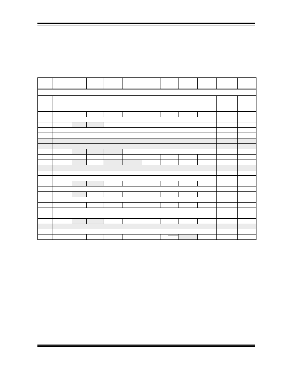
TABLE 2-1:
SPECIAL FUNCTION REGISTER SUMMARY
Address
Name
Bit 7
Bit 6
Bit 5
Bit 4
Bit 3
Bit 2
Bit 1
Bit 0
Value on
POR, BOR
Details on
page:
Bank 0
00h(1)
INDF
Addressing this location uses contents of FSR to address data memory (not a physical register) 0000 0000
01h
TMR0
Timer0 Module’s Register
xxxx xxxx
02h(1)
PCL
Program Counter's (PC) Least Significant Byte
0000 0000
03h(1)
STATUS
IRP
RP1
RP0
TO
PD
Z
DC
C
0001 1xxx
04h(1)
FSR
Indirect Data Memory Address Pointer
xxxx xxxx
05h
PORTA
—
PORTA Data Latch when written: PORTA pins when read
--0x 0000
06h
PORTB
PORTB Data Latch when written: PORTB pins when read
xxxx xxxx
07h
PORTC
PORTC Data Latch when written: PORTC pins when read
xxxx xxxx
08h
—
Unimplemented
—
09h
—
Unimplemented
—
0Ah(1,2)
PCLATH
—
Write Buffer for the upper 5 bits of the Program Counter
---0 0000
0Bh(1)
INTCON
GIE
PEIE
TMR0IE
INTE
RBIE
TMR0IF
INTF
RBIF
0000 000x
0Ch
PIR1
—ADIF
—
SSPIF
CCP1IF
TMR2IF
TMR1IF
-0-- 0000
0Dh
—
Unimplemented
—
0Eh
TMR1L
Holding Register for the Least Significant Byte of the 16-bit TMR1 Register
xxxx xxxx
0Fh
TMR1H
Holding Register for the Most Significant Byte of the 16-bit TMR1 Register
xxxx xxxx
10h
T1CON
—
T1CKPS1
T1CKPS0 T1OSCEN
T1SYNC
TMR1CS
TMR1ON
--00 0000
11h
TMR2
Timer2 Module’s Register
0000 0000
12h
T2CON
—
TOUTPS3 TOUTPS2 TOUTPS1 TOUTPS0 TMR2ON
T2CKPS1
T2CKPS0 -000 0000
13h
SSPBUF
Synchronous Serial Port Receive Buffer/Transmit Register
xxxx xxxx
14h
SSPCON
WCOL
SSPOV
SSPEN
CKP
SSPM3
SSPM2
SSPM1
SSPM0
0000 0000
15h
CCPR1L
Capture/Compare/PWM Register (LSB)
xxxx xxxx
16h
CCPR1H
Capture/Compare/PWM Register (MSB)
xxxx xxxx
17h
CCP1CON
—
CCP1X
CCP1Y
CCP1M3
CCP1M2
CCP1M1
CCP1M0
--00 0000
18h-1Dh
—
Unimplemented
—
1Eh
ADRES
A/D Result Register
xxxx xxxx
1Fh
ADCON0
ADCS1
ADCS0
CHS2
CHS1
CHS0
GO/DONE
—ADON
0000 00-0
Legend:
x
= unknown, u = unchanged, q = value depends on condition, - = unimplemented, read as ‘0’, r = reserved.
Shaded locations are unimplemented, read as ‘0’.
Note
1:
These registers can be addressed from any bank.
2:
The upper byte of the program counter is not directly accessible. PCLATH is a holding register for the PC<12:8> whose
contents are transferred to the upper byte of the program counter.
3:
This bit always reads as a ‘1’.
发布紧急采购,3分钟左右您将得到回复。
相关PDF资料
XF2R34154A
CONN FPC 34POS 0.5MM PITCH SMD
XF2R24154A
CONN FPC 24POS 0.5MM PITCH SMD
PIC18F45K20-I/ML
IC PIC MCU FLASH 16KX16 44QFN
PIC18F14K50-I/SO
IC PIC MCU FLASH 8KX16 20-SOIC
PIC16F628A-I/SS
IC MCU FLASH 2KX14 EEPROM 20SSOP
PIC18LF43K22-I/PT
IC PIC MCU 8KB FLASH 44TQFP
DSPIC33FJ16MC101-I/SO
IC DSP 16BIT 16KB 20SOIC
PIC12C672-04I/SM
IC MCU OTP 2KX14 A/D 8-SOIJ
相关代理商/技术参数
PIC16F72-I/MLG
功能描述:8位微控制器 -MCU 3.5KB 128 RAM 22 I/O Lead Free Package RoHS:否 制造商:Silicon Labs 核心:8051 处理器系列:C8051F39x 数据总线宽度:8 bit 最大时钟频率:50 MHz 程序存储器大小:16 KB 数据 RAM 大小:1 KB 片上 ADC:Yes 工作电源电压:1.8 V to 3.6 V 工作温度范围:- 40 C to + 105 C 封装 / 箱体:QFN-20 安装风格:SMD/SMT
PIC16F72-I/SO
功能描述:8位微控制器 -MCU 3.5KB 128 RAM 22 I/O
RoHS:否 制造商:Silicon Labs 核心:8051 处理器系列:C8051F39x 数据总线宽度:8 bit 最大时钟频率:50 MHz 程序存储器大小:16 KB 数据 RAM 大小:1 KB 片上 ADC:Yes 工作电源电压:1.8 V to 3.6 V 工作温度范围:- 40 C to + 105 C 封装 / 箱体:QFN-20 安装风格:SMD/SMT
PIC16F72-I/SO
制造商:Microchip Technology Inc 功能描述:8BIT FLASH MCU SMD 16F72 SOIC28
PIC16F72-I/SOG
功能描述:8位微控制器 -MCU 3.5KB 128 RAM 22 I/O Lead Free Package RoHS:否 制造商:Silicon Labs 核心:8051 处理器系列:C8051F39x 数据总线宽度:8 bit 最大时钟频率:50 MHz 程序存储器大小:16 KB 数据 RAM 大小:1 KB 片上 ADC:Yes 工作电源电压:1.8 V to 3.6 V 工作温度范围:- 40 C to + 105 C 封装 / 箱体:QFN-20 安装风格:SMD/SMT
PIC16F72-I/SP
功能描述:8位微控制器 -MCU 3.5KB 128 RAM 22 I/O
RoHS:否 制造商:Silicon Labs 核心:8051 处理器系列:C8051F39x 数据总线宽度:8 bit 最大时钟频率:50 MHz 程序存储器大小:16 KB 数据 RAM 大小:1 KB 片上 ADC:Yes 工作电源电压:1.8 V to 3.6 V 工作温度范围:- 40 C to + 105 C 封装 / 箱体:QFN-20 安装风格:SMD/SMT
PIC16F72-I/SP
制造商:Microchip Technology Inc 功能描述:IC 8BIT FLASH MCU 16F72 SDIL28
PIC16F72-I/SS
功能描述:8位微控制器 -MCU 3.5KB 128 RAM 22 I/O
RoHS:否 制造商:Silicon Labs 核心:8051 处理器系列:C8051F39x 数据总线宽度:8 bit 最大时钟频率:50 MHz 程序存储器大小:16 KB 数据 RAM 大小:1 KB 片上 ADC:Yes 工作电源电压:1.8 V to 3.6 V 工作温度范围:- 40 C to + 105 C 封装 / 箱体:QFN-20 安装风格:SMD/SMT
PIC16F72-I/SS
制造商:Microchip Technology Inc 功能描述:8BIT FLASH MCU SMD 16F72 SSOP28